We are ready to help you
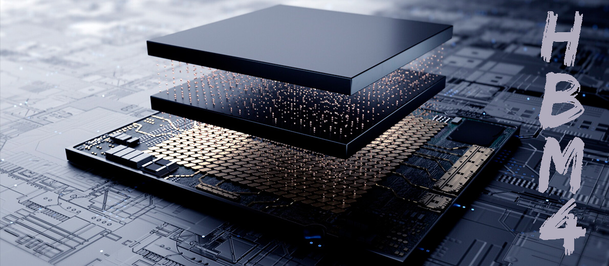
HBM4: The last frontier before the “Memory Wall”. A full technological breakdown of the architecture and manufacturing wars
In the mid-2020s, the high-performance computing (HPC) and artificial intelligence industry ran into a fundamental physical problem. Moore’s law, which predicted a doubling of the number of transistors, kept working, but a new imbalance appeared: GPU compute cores became so fast that the memory subsystem could no longer feed them data in time. This phenomenon was called the Memory Wall.
If in the HBM2e and HBM3 era the bottleneck was capacity, then by the time architectures like NVIDIA Rubin and AMD Instinct MI400 were announced, the critical factor became bandwidth and the energy efficiency of transferring a single bit of information. The industry’s answer was the HBM4 (High Bandwidth Memory Generation 4) standard — a technology that changes not just speed but the very paradigm of chip design.
A detailed analysis of the architecture, manufacturing challenges, and market prospects of HBM4 is presented below.
Part 1. Architectural revolution: Why change the rules of the game?
The transition from HBM3e to HBM4 is not an evolutionary frequency bump like in the GDDR standard. It is a radical change in the interface architecture, formalized in JEDEC standards (JESD270-4).
1.1. Bus expansion: From 1024 to 2048 bits
Up to and including the HBM3e generation, each memory stack (DRAM stack) communicated with the processor (Host GPU/ASIC) via a 1024-bit interface. To increase bandwidth, engineers had to constantly push the memory clock higher. However, the physics of conductors are unforgiving: increasing frequency leads to a nonlinear increase in heat dissipation and signal integrity issues.
With HBM4, the industry went “wider”:
- Interface width: Doubled to 2048 bits per stack.
- Meaning of the change: Doubling the number of data channels makes it possible to lower the memory clock while simultaneously increasing overall bandwidth.
- Result: The peak bandwidth of a single stack exceeds 1.5–1.65 TB/s (terabytes per second). For comparison, a typical DDR5 module in a consumer PC delivers around 60–70 GB/s. A single HBM4 stack is more than 20 times faster, and there can be 8 or even 12 such stacks on a single GPU.
1.2. 16-high stack (16-Hi Stack)
The HBM4 standard was initially designed for vertical integration of 16 DRAM layers (16-Hi). In previous generations, 8-Hi and 12-Hi configurations were standard. Moving to 16 layers sharply increases memory density. A single HBM4 stack can have a capacity of 48 GB or even 64 GB. This is critical for LLMs (Large Language Models), where model parameters (weights) must fully fit into VRAM for efficient inference.
Part 2. Base die: Memory gets smart
The most significant change in HBM4, often missed in surface-level overviews, is the transformation of the Base Die.
2.1. Moving away from memory process nodes
In HBM3e, the base die, which serves as the foundation of the stack and the router for signals, was manufactured using the same process technology as the memory itself (DRAM process). This is cheap but imposes limitations on logic.
In HBM4, the base die is manufactured at external foundries such as TSMC using logic process nodes:
- 12nm FFC+ (FinFET Compact): For more economical solutions.
- 5nm (N5): For high-performance solutions.
2.2. Why put logic into memory?
Using a 5-nanometer process for the base layer opens the era of Processing-In-Memory (PIM) or Near-Memory Computing.
- Intelligent routing: More complex controllers inside the memory can optimize data flows.
- RAS (Reliability, Availability, Serviceability): Built-in error correction mechanisms (ECC) become much stronger, which is necessary at such extreme bit density.
- Lower power consumption: A logic process node allows reducing the interface supply voltage, which helps offset the increase in the number of channels.
This turns HBM4 from a simple “storage” into an active coprocessor that takes over routine operations, offloading the main data bus.
Part 3. Manufacturing war: Hybrid Bonding vs MR-MUF
The main intrigue and major misconceptions lie in packaging technologies. In the original article it was claimed that the industry had completely abandoned micro-bumps in favor of hybrid bonding. That is not quite true — the reality is much more complex and interesting.
3.1. The problem of height and heat
A 16-layer silicon stack is physically taller than an 8- or 12-layer one. However, JEDEC specifications strictly limit the total module height (720 microns) so that it fits under standard heatsinks and into 2.5D packaging architectures (CoWoS).
- Task: Make the silicon layers themselves thinner and reduce the gaps between them.
- Risk: Thinned wafers become fragile and warp under heat, leading to warpage and breakage during assembly.
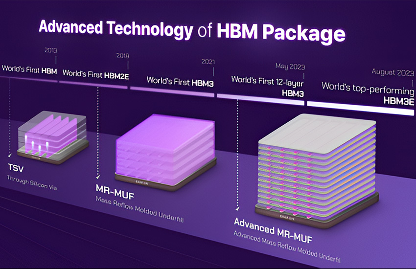
3.2. SK Hynix strategy: MR-MUF evolution
SK Hynix, which holds more than 50% of the HBM market and is the main supplier for NVIDIA, has not abandoned bumps in HBM4. They use an improved Advanced MR-MUF (Mass Reflow Molded Underfill) technology.
- Essence of the method: Layers are connected with micro-bumps (tin-lead solder balls), and the space between them is filled with a special liquid compound (mold), which then solidifies.
- Advantage: MR-MUF provides better heat dissipation (the compound works as a thermal conductor) and reduces mechanical stress on fragile dies during assembly.
- HBM4 implementation: SK Hynix managed to shrink bump size and pitch enough to fit 16 layers within the standard height while maintaining reliability and a high yield.
3.3. Samsung strategy: Betting on Hybrid Bonding
Samsung Electronics, trying to catch up with its competitor, is actively investing in Hybrid Bonding (HCB — Hybrid Copper Bonding).
- Essence of the method: Direct “copper-to-copper” bonding without solder (bumps). Silicon layers are polished to a near-perfect mirror finish and bonded using van der Waals forces followed by annealing.
- Advantage: Enables minimal stack thickness and superior electrical conductivity.
- Drawbacks: Extremely complex manufacturing. A speck of dust just a few nanometers in size between layers can ruin the entire stack. This makes the technology very expensive and not yet suitable for true high-volume mass production.
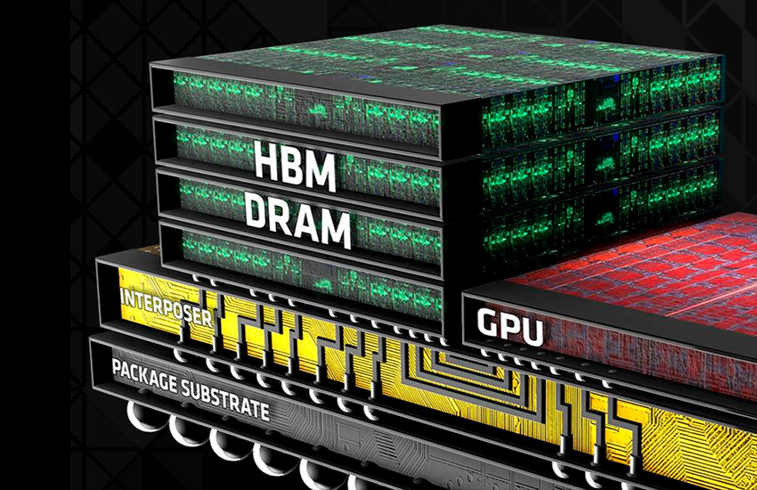
Part 4. Integration and ecosystem: CoWoS and interposers
By itself, HBM4 memory is useless without a processor. Their union happens on a substrate using CoWoS (Chip-on-Wafer-on-Substrate) technology, which TSMC is pushing forward.
4.1. The interposer problem
HBM4 with its 2048-bit bus requires twice as many pads on the interposer (the silicon bridge connecting memory and GPU).
- Standard interposers (reticle limit) have already reached their maximum size.
- For HBM4 and new GPUs, CoWoS-L (Local Silicon Interconnect) and CoWoS-R are used. These technologies make it possible to “stitch” several interposers together, creating gigantic packages that exceed the photomask size by 3–4 times.
4.2. The role of TSMC
Taiwanese giant TSMC is becoming not just a chip maker but a system integrator. Its ability to reliably “assemble” a GPU (manufactured on 3nm) and an HBM4 base die (manufactured on 5nm) into a single package largely determines the success of NVIDIA and AMD.
Part 5. Energy efficiency and physics
Why is HBM4 so important for the environmental impact of data centers?
5.1. The pJ/bit metric
The key efficiency metric is how many picojoules of energy are spent to transmit one bit of data. In GDDR6X this number is high due to the long traces on the PCB. In HBM4, thanks to microscopic distances (through TSVs — Through-Silicon Vias) and a wide bus, this figure drops to record lows.
5.2. Thermal throttling
Despite its efficiency, packing 16 layers together creates enormous heat density. If HBM3e was already reaching 85–90°C, HBM4 requires even more advanced cooling systems. This is pushing servers toward direct liquid cooling (Direct Liquid Cooling), as air can no longer cope with cooling packages that consume 1000–1200 W (GPU + HBM).
Part 6. Market realities and timelines (Fact-Checking)
Based on data as of the end of 2025, the market situation looks as follows:
- Sampling: SK Hynix and Samsung have indeed started shipping 12-Hi and 16-Hi HBM4 engineering samples to key partners (NVIDIA, AMD, Google) in the second half of 2025. This is required for qualification and tuning of memory controllers in new GPUs.
- Volume production: Full-scale ramp-up for commercial sales is scheduled for the first half of 2026.
- First products: The first devices with HBM4 are expected to be accelerators of the NVIDIA Rubin (R100) series and refreshed AMD Instinct MI450 lineups, which are anticipated to be announced in 2026.
The claim that HBM4 is already being sold in commercial products in 2025 is an exaggeration. In 2025, HBM3e still reigns supreme (in H200 and Blackwell B200 accelerators).
Part 7. HBM4 vs GDDR7: Why not for gamers?
A common question from users: “When will HBM4 appear in my GeForce RTX 6090?” The answer is: never. Here’s why:
- Cost: A single HBM3e/4 stack costs tens of times more than a GDDR7 chip of the same capacity. The complexity of CoWoS packaging makes producing consumer graphics cards with HBM economically impractical.
- GDDR7: The new GDDR7 graphics memory standard has also entered the market. It offers speeds of up to 32–40 Gbps per pin and uses PAM3 encoding. For gaming workloads where you don’t need simultaneous access to 192 GB of memory with 6 TB/s of bandwidth, GDDR7 is the ideal balance of price and performance.
HBM4 will remain the domain of the enterprise segment, supercomputers, and AI clusters.
Conclusion
HBM4 is a triumph of engineering over physical limitations. Moving to a 2048-bit bus, introducing 5nm logic process nodes into the base die, and mastering the packaging of 16 silicon layers into 700 microns of height all help postpone the “death of Moore’s law” for a few more years.
For the AI industry, this means the ability to train trillion-parameter models much faster and more efficiently. However, the production complexity makes this resource strategic and extremely expensive. The battle for HBM4 supply in 2026 will be a defining factor in the leadership struggle between tech giants from the US and Asia.
Expert conclusion from HYPERPC
At HYPERPC, we closely follow cutting-edge technologies. The emergence of HBM4 standard memory is a tectonic shift that, although it starts in data-center server racks, inevitably sets the direction for the development of the entire industry.
Today, technologies like HBM4 power the neural networks that help us design, optimize, and create better computers for you. And while HBM4 will not appear in home gaming rigs any time soon due to its specifics and cost, the innovations it drives (new cooling methods, data-bus optimization, advanced chip-packaging technologies) will eventually be adapted and transformed for the High-End Desktop (HEDT) segment.
For our clients — professionals, content creators, and enthusiasts — we at HYPERPC always choose the best available options. Whether it’s cutting-edge GDDR7-based solutions or extreme workstations with professional NVIDIA RTX accelerators, we guarantee that your computer will be ready for tomorrow’s challenges. Technologies change, but our commitment to excellence and maximum performance remains unchanged.
HYPERPC — Plug into the future today.